| CPC H01L 25/50 (2013.01) [C09J 129/14 (2013.01); C09J 167/02 (2013.01); C09J 171/02 (2013.01); C09J 183/04 (2013.01); H01L 21/304 (2013.01); H01L 21/6835 (2013.01); H01L 21/76898 (2013.01); H01L 21/7806 (2013.01); H01L 24/29 (2013.01); H01L 24/83 (2013.01); H01L 2224/2919 (2013.01); H01L 2224/83855 (2013.01); H01L 2924/0675 (2013.01); H01L 2924/0685 (2013.01); H01L 2924/0715 (2013.01)] | 21 Claims |
|
1. A method of manufacturing a semiconductor device, the method comprising:
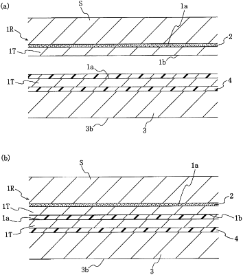
preparing a reinforced wafer having a laminated structure, the laminated structure comprising a wafer including an element forming surface and a back surface opposite from the element forming surface, a supporting substrate, and a temporary adhesive layer located between the element forming surface side of the wafer and the supporting substrate;
forming a thinned wafer by grinding the wafer in the reinforced wafer from the back surface side of the wafer;
bonding an element forming surface side of a base wafer to the back surface side of the thinned wafer of the reinforced wafer via an adhesive, so that the temporary adhesive layer is located between the element forming surface side of the thinned wafer and the supporting substrate, and the adhesive is located between the element forming surface side of the base wafer and the back surface side of the thinned wafer, the base wafer including the element forming surface and a back surface opposite from the element forming surface; and
removing the supporting substrate by releasing a temporary adhesion in the temporary adhesive layer located between the supporting substrate and the thinned wafer in the reinforced wafer;
wherein a temporary adhesive for forming the temporary adhesive layer contains a polyvalent vinyl ether compound, a compound including two or more hydroxy groups or carboxy groups that are capable of forming an acetal bond by reacting with a vinyl ether group of the polyvalent vinyl ether compound so as to form a polymer with the polyvalent vinyl ether compound, and a thermoplastic resin,
the temporary adhesive for forming the temporary adhesive layer is coated on the supporting substrate to form the temporary adhesive coating, and
the adhesive contains a polymerizable group-containing polyorganosilsesquioxane.
|