| CPC H01L 25/167 (2013.01) [H01L 24/95 (2013.01); H01L 25/0753 (2013.01); H01L 25/165 (2013.01); H01L 27/0203 (2013.01); H01L 27/124 (2013.01); H01L 27/1244 (2013.01); H01L 33/0008 (2013.01); H01L 33/06 (2013.01); H01L 33/08 (2013.01); H01L 33/20 (2013.01); H01L 33/30 (2013.01); H01L 33/44 (2013.01); H01L 33/486 (2013.01); H01L 33/52 (2013.01); H01L 33/54 (2013.01); H01L 33/56 (2013.01); H01L 33/60 (2013.01); H01L 33/62 (2013.01); H01L 2924/0002 (2013.01); H01L 2924/12041 (2013.01); H01L 2924/12042 (2013.01); H01L 2924/12044 (2013.01); H01L 2933/005 (2013.01); H01L 2933/0025 (2013.01); H01L 2933/0033 (2013.01); H01L 2933/0066 (2013.01)] | 15 Claims |
|
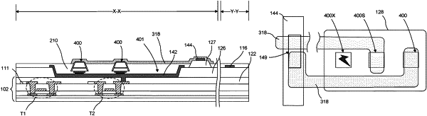
1. A display panel pixel structure comprising:
a substrate including a tie line and a planarization layer over the tie line;
a plurality of light emitting diode (LEDs) over the planarization layer, the plurality of LEDs including a first pair of redundant LEDs within a first subpixel and a second pair of LEDs within a second subpixel;
a passivation layer over the substrate and laterally around the plurality of LEDs; and
a top conductive electrode layer over the passivation layer that electrically connects a first LED of the first pair of LEDs and a second LED of the second pair of LEDs with the tie line.
|