| CPC H01L 25/0655 (2013.01) [H01L 21/56 (2013.01); H01L 21/561 (2013.01); H01L 21/563 (2013.01); H01L 21/568 (2013.01); H01L 21/6835 (2013.01); H01L 23/3128 (2013.01); H01L 23/3135 (2013.01); H01L 23/3185 (2013.01); H01L 23/5383 (2013.01); H01L 23/5385 (2013.01); H01L 23/5386 (2013.01); H01L 24/14 (2013.01); H01L 24/16 (2013.01); H01L 24/73 (2013.01); H01L 24/97 (2013.01); H01L 25/50 (2013.01); H01L 21/486 (2013.01); H01L 23/49816 (2013.01); H01L 2221/68345 (2013.01); H01L 2224/1403 (2013.01); H01L 2224/16225 (2013.01); H01L 2224/16227 (2013.01); H01L 2224/18 (2013.01); H01L 2224/73204 (2013.01); H01L 2224/81005 (2013.01); H01L 2224/95001 (2013.01); H01L 2224/97 (2013.01)] | 20 Claims |
|
1. An electronic device comprising:
a signal redistribution structure comprising a redistribution structure top side, a redistribution structure bottom side, and redistribution structure lateral sides, wherein the signal redistribution structure is coreless;
an electronic component comprising a component top side, a component bottom side, and component lateral sides, wherein the component top side is coupled to the component bottom side;
a vertical interconnect structure coupled to the redistribution structure bottom side at a position that is laterally offset from the electronic component;
a component interconnect structure that is coupled to the component top side and to the redistribution structure bottom side, such that the electronic component is electrically coupled to the signal redistribution structure through at least the component interconnect structure;
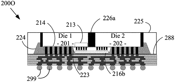
a semiconductor die comprising a die top side, a die bottom side, and die lateral sides;
a first die interconnect structure coupled to the redistribution structure top side and to the die bottom side, such that the semiconductor die is electrically coupled to the vertical interconnect structure;
a second die interconnect structure coupled to the redistribution structure top side and to the die bottom side, such that the semiconductor die is electrically coupled to the electronic component;
an underfill material between the die bottom side and the redistribution structure top side, wherein the underfill material laterally surrounds the first die interconnect structure and the second die interconnect structure; and
an upper encapsulating material that laterally surrounds the semiconductor die and the underfill material.
|