| CPC H01L 23/544 (2013.01) [H01L 22/12 (2013.01); H01L 2223/54426 (2013.01)] | 20 Claims |
|
1. A metrology target for use in measuring misregistration between layers of a
semiconductor device comprising:
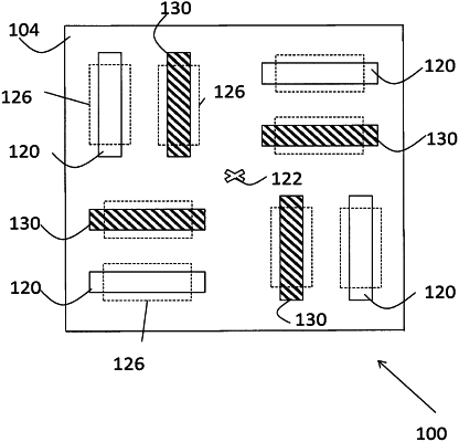
a first target structure placed on a first layer of a semiconductor device, said first target structure comprising a first plurality of unitary elements respectively located in at least four regions of said first target structure, said first plurality of elements being rotationally symmetric with respect to a first center of symmetry; and
at least a second target structure placed on at least a second layer of said semiconductor device, said second target structure comprising a second plurality of elements respectively located in at least four regions of said second target structure, said second plurality of elements being rotationally symmetric with respect to a second center of symmetry,
said second center of symmetry being designed to be axially aligned with said first center of symmetry and corresponding ones of said second plurality of elements being located adjacent corresponding ones of said first plurality of elements in said at least four regions in a non-surrounding arrangement, when said first and second layers are placed one on top of another, wherein a plurality of measurement regions of interest are defined such that one of the plurality of measurement regions of interest is defined with respect to each of said first plurality of elements and second plurality of elements, and wherein a length along a long dimension of said first plurality of elements is shorter than a length along a long dimension of said second plurality of elements.
|