|
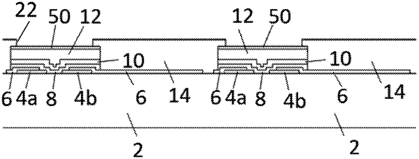
1. A device, comprising: a stack of layers defining at least: a source-drain conductor pattern at a first level of the stack; and one or more semiconductor channels in respective semiconductor channel regions, connecting a pair of parts of the source-drain conductor pattern, and capacitively coupled via a dielectric to a coupling conductor of a gate conductor pattern at a second level of the stack; wherein the stack comprises: at least two insulator patterns; wherein a first insulator pattern of the at least two insulator patterns occupies at least the one or more semiconductor channel regions to provide the dielectric; and a second insulator pattern of the at least two insulator patterns defines one or more windows in at least the one or more semiconductor channel regions through which the gate conductor pattern contacts the first insulator pattern other than via the insulator pattern; wherein the second insulator pattern overlaps the first insulator pattern outside the one or more semiconductor channel regions; wherein the gate conductor pattern is formed over the at least two insulator patterns; and the coupling conductor of the gate conductor pattern is formed at least over the whole area of the first insulator pattern.
|