| CPC H01L 23/3178 (2013.01) [H01L 21/565 (2013.01); H01L 21/67288 (2013.01); H01L 23/367 (2013.01); H01L 23/373 (2013.01)] | 26 Claims |
|
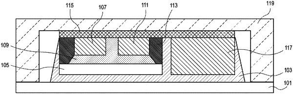
1. A device, comprising:
a first die;
a plurality of chiplets above the first die;
a first underfill material beneath the chiplets;
a gap fill material between the chiplets, the gap fill material different from the first underfill material;
an interface region between the first underfill material and the gap fill material; and
a mold material adjacent sides of the chiplets, wherein the gap fill material is different from the mold material.
|