| CPC H01L 21/76837 (2013.01) [H01J 37/32183 (2013.01); H01J 37/32449 (2013.01); H01J 37/32522 (2013.01); H01J 37/32568 (2013.01); H01L 21/0217 (2013.01); H01L 21/02115 (2013.01); H01L 21/02164 (2013.01); H01L 21/67248 (2013.01); H01L 21/6833 (2013.01); H01L 21/76224 (2013.01); H01J 2237/3321 (2013.01)] | 20 Claims |
|
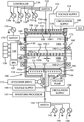
1. A gapfill deposition method comprising:
generating a plasma above a substrate from a gapfill precursor by applying, at the same time, a first RF bias and a second RF bias to an electrostatic chuck supporting the substrate to deposit a gapfill within at least one feature within the substrate, the at least one feature extending a depth from the substrate surface to a bottom surface, the at least one feature having an opening width at the substrate surface defined by a first sidewall and a second sidewall.
|