| CPC H01L 21/67132 (2013.01) [H01L 21/3043 (2013.01); H01L 21/6836 (2013.01); H01L 21/78 (2013.01)] | 16 Claims |
|
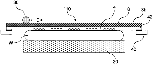
14. A protective sheeting for use in processing a semiconductor-sized wafer, the protective sheeting comprising:
a protective film; and
a cushioning layer attached to a back surface of the protective film, the cushioning layer being curable by an external stimulus so that the cushioning layer hardens at least to some degree upon application of the external stimulus,
wherein, at least in a central area of the protective sheeting, no adhesive is applied to a front surface and a back surface of the protective sheeting, the central area having an outer diameter which is equal to or larger than an outer diameter of the semiconductor-sized wafer, and
a substantially annular adhesive layer is applied to an outer peripheral portion of a front surface of the protective film opposite to the back surface thereof.
|