| CPC H01L 21/67121 (2013.01) [B23K 26/0622 (2015.10); B23K 26/382 (2015.10); H01L 21/486 (2013.01); H01L 23/3121 (2013.01); H01L 23/49827 (2013.01)] | 18 Claims |
|
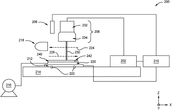
1. A system for laser patterning a semiconductor device substrate, comprising:
a diode-pumped solid-state laser source configured to generate a pulsed laser beam, the laser source comprising a slab gain medium, the laser source further characterized by:
a pulse energy between about 0.25 mJ and about 10 mJ;
a pulse width between about 1 ns and about 4000 ns; and
a pulse frequency between about 1 kHz and about 200 kHz;
a galvanometer optical scanner;
a first telecentric lens having a field of view (FOV) with lateral dimensions substantially equal to or greater than about 137 mm, the first telecentric lens having a working distance between about 30 mm and about 500 mm; and
a second telecentric lens having FOV with lateral dimensions substantially equal to or greater than about 137 mm and a working distance between about 30 mm and about 500 mm.
|