| CPC H01L 21/67092 (2013.01) [H01L 21/4825 (2013.01); H01L 21/565 (2013.01); H01L 21/78 (2013.01); H01L 23/562 (2013.01); H01L 2223/5446 (2013.01)] | 6 Claims |
|
1. A method for packaging electronic devices, comprising:
forming electronic devices on a semiconductor wafer;
separating the electronic devices from one another by cutting through the semiconductor wafer in scribe lanes on the semiconductor wafer between the electronic devices;
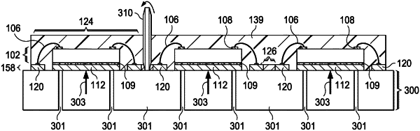
mounting the electronic devices on a package substrate, the package substrate carrying an array of electronic devices, the electronic devices spaced from one another on the package substrate by saw streets defined between the electronic devices;
electrically coupling bond pads on the electronic devices to leads on the package substrate;
covering the electronic devices and portions of the package substrate with mold compound;
placing the array of electronic devices on a device chuck in a process chamber;
increasing a pressure in the process chamber to a pressure greater than one atmosphere;
sawing through the mold compound and the package substrate along the saw streets between the electronic devices to separate molded electronic devices one from another; and
removing the molded electronic devices from the process chamber.
|