| CPC H01F 27/32 (2013.01) [H01F 27/24 (2013.01); H01F 27/2823 (2013.01); H01F 27/29 (2013.01); H01F 41/061 (2016.01); H01F 41/12 (2013.01)] | 20 Claims |
|
1. An electronic component comprising:
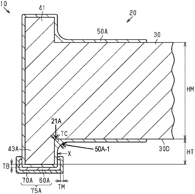
a component body including a core having a winding core part;
an insulating layer that comprises a material having a higher insulating property than the component body and that partially covers a surface of the component body; and
an electrode that is stacked on a surface of the insulating layer;
wherein the electrode includes a base electrode that is stacked on the surface of the insulating layer and a plating layer that is stacked on a surface of the base electrode, and the insulating layer has a larger surface area than the electrode and the electrode is stacked at a position separated from an edge of the insulating layer, the edge of the insulating layer being present along the winding core part of the core at a position spaced from a flange part so that a portion of the winding core part is exposed beginning at the edge of the insulating layer.
|