| CPC G11B 20/10259 (2013.01) [G11B 20/10462 (2013.01); G11B 20/1217 (2013.01); G11B 20/1803 (2013.01); G11C 13/04 (2013.01); G11B 2020/1237 (2013.01)] | 14 Claims |
|
1. A storage device comprising:
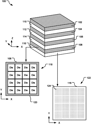
a layer stack including at least:
a memory layer including a plurality of memory cells; and
an optical control layer positioned adjacent to the memory layer in the layer stack, the optical control layer being adapted to receive and transmit optically-encoded read/write signals and effect read and write operations to the plurality of memory cells through an electrical interface; and
a plurality of wave division multiplexers (WDMs) each being positioned to couple optical signals delivered by a bus waveguide to a respective optical-electrical conversion element coupled to the memory layer, the plurality of WDMs including:
a first subset of WDMs dedicated to transporting write signals from the optical control layer to the memory layer; and
a second subset of WDMs dedicated to transporting read signals from the memory layer to the optical control layer, each of the WDMs in the first subset and in the second subset being tuned for operation at a different wavelength to collectively support parallel transport of multiple read streams and multiple write streams within the bus waveguide.
|