| CPC G06F 13/4234 (2013.01) [G06F 1/08 (2013.01); G06F 13/1689 (2013.01); G06F 13/4282 (2013.01); G11C 8/06 (2013.01); G11C 8/18 (2013.01)] | 22 Claims |
|
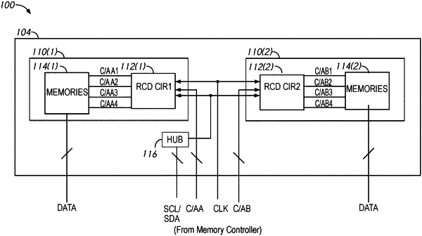
1. An apparatus comprising:
a first register clock driver configured to receive first configuration data in first subchannel command and address information corresponding to a channel from a memory controller via a first command and address bus, wherein the first register clock driver is further configured to receive second configuration data, wherein the first register clock driver is configured to update parameters set by the second configuration data with updates provided via the first configuration data;
a second register clock driver configured to receive second subchannel command and address information corresponding to the channel from the memory controller via a second command and address bus, wherein the second register clock driver is further configured to receive the second configuration data; and
a control plane hub configured to receive the second configuration data from a memory controller via a serial data bus and to provide the second configuration data to the first register clock driver and to the second register clock driver.
|