| CPC G02F 1/136209 (2013.01) [G02F 1/13398 (2021.01); G02F 1/133368 (2021.01); G02F 1/133553 (2013.01); G02F 1/133616 (2021.01); G09G 3/3607 (2013.01); G02F 1/133614 (2021.01)] | 20 Claims |
|
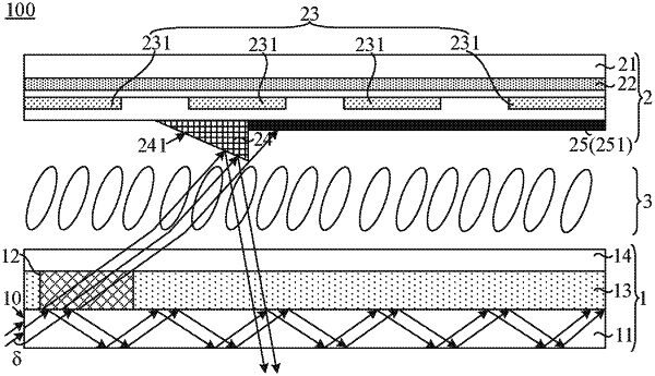
1. A display panel having a display area including a plurality of sub-pixel regions, the display panel comprising:
a first substrate and a second substrate that are oppositely arranged; and
a liquid crystal layer disposed between the first substrate and the second substrate, wherein
the first substrate includes:
a first base having a first side facing the second substrate and a plurality of second sides intersecting the first side; and
a light extraction portion and a light conversion portion that are disposed on the first side and located in each sub-pixel region, a refractive index of the light extraction portion being greater than or equal to a refractive index of the first base, a refractive index of a portion of the light conversion portion in direct contact with the first base being less than the refractive index of the first base, and at least one second side being a light incident surface;
the second substrate includes:
a second base;
at least one light reflecting structure and at least one light absorbing structure that are disposed at a side of the second base facing the first substrate and located in a sub-pixel region of the plurality of sub-pixel regions; at least one side of the light reflecting structure being provided with the light absorbing structure; and
the light reflecting structure is configured to reflect light that exits from the light extraction portion, passes through the liquid crystal layer, and is incident onto the light reflecting structure, so that the reflected light passes through the first substrate to exit; the light absorbing structure is configured to absorb light that exits from the light extraction portion, passes through the liquid crystal layer, and is incident onto the light absorbing structure.
|