US 11,675,234 B2
Display apparatus and method of manufacturing the same
Jaekyung Go, Yongin-si (KR); Eunjae Na, Yongin-si (KR); Minjun Jo, Yongin-si (KR); and Hyunmin Hwang, Yongin-si (KR)
Assigned to Samsung Display Co., Ltd., Yongin-si (KR)
Filed by SAMSUNG DISPLAY CO., LTD., Yongin-si (KR)
Filed on Dec. 13, 2021, as Appl. No. 17/549,604.
Application 17/549,604 is a division of application No. 16/696,542, filed on Nov. 26, 2019, granted, now 11,199,746.
Application 16/696,542 is a continuation of application No. 15/997,650, filed on Jun. 4, 2018, granted, now 10,520,774, issued on Dec. 31, 2019.
Application 15/997,650 is a continuation of application No. 15/273,569, filed on Sep. 22, 2016, granted, now 9,989,811, issued on Jun. 5, 2018.
Claims priority of application No. 10-2015-0166409 (KR), filed on Nov. 26, 2015.
Prior Publication US 2022/0100013 A1, Mar. 31, 2022
This patent is subject to a terminal disclaimer.
Int. Cl. G02F 1/1339 (2006.01); G02F 1/1333 (2006.01); H01L 51/52 (2006.01); H01L 27/32 (2006.01)
CPC G02F 1/1339 (2013.01) [G02F 1/133351 (2013.01); H01L 27/323 (2013.01); H01L 51/5246 (2013.01); G02F 2201/503 (2013.01)] 12 Claims
OG exemplary drawing
 
1. A display apparatus comprising:
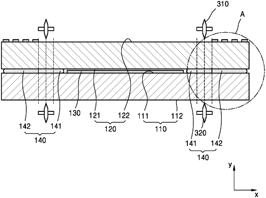
a first substrate comprising a first inner surface and a first outer surface opposite to the first inner surface;
a second substrate comprising a second inner surface facing the first inner surface and a second outer surface opposite to the second inner surface;
a display element between the first inner surface and the second inner surface, the display element comprising a light emitting diode and a thin-film transistor; and
a sealing element located between the first and second substrates, and surrounding the display element;
wherein the first substrate further comprises a first side surface connecting the first inner surface and the first outer surface, the first side surface comprising a first flat surface and a first curved surface.