| CPC G01S 7/35 (2013.01) [G01S 7/282 (2013.01); H03F 3/245 (2013.01); H03K 5/00006 (2013.01); H03F 2200/451 (2013.01)] | 18 Claims |
|
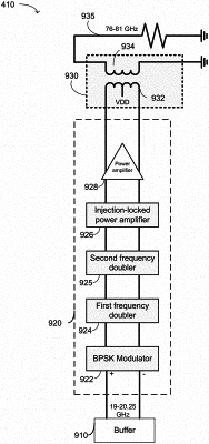
1. A semiconductor device, comprising:
a transmitter, comprising:
a first circuit configured to receive a differential input signal having a first frequency and provide a differential modulated signal having the first frequency and a first clock phase, the first circuit comprising:
an injection-locked ring oscillator configured to generate a plurality of phase shifts; and
a switching circuit configured to select the first clock phase from the plurality of phase shifts;
a second circuit comprising one or more frequency multipliers, wherein the one or more frequency multipliers is configured to receive the differential modulated signal and provide a differential second signal having a second frequency greater than the first frequency and having a second clock phase; and
an output transformer configured to receive the differential second signal and transform the differential second signal to a single-ended output signal.
|