| CPC G01R 31/318335 (2013.01) [G01R 31/002 (2013.01); G06F 1/04 (2013.01); G06F 7/64 (2013.01); G06F 30/347 (2020.01)] | 20 Claims |
|
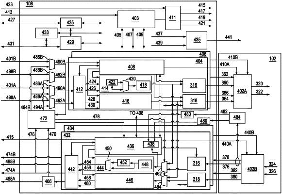
1. An embedded physical layer (EPHY), comprising:
a glue hardware portion; and
a logic portion for communicating with a device under test (DUT) through the glue hardware portion, wherein the logic portion comprises:
a plurality of transmission blocks that each includes:
a transmission remote monitor and maintenance interface (RMMI) multiplexer (MUX) and wrapper;
a first low speed logic block of a first speed; and
a first high speed logic block of a second speed, wherein the second speed is greater than the first speed, wherein the transmission RMMI MUX and wrapper is configured to input a data signal and a clock signal to the first low speed logic block, wherein the transmission RMMI MUX and wrapper is configured to input a data signal and a clock signal to the first high speed logic block, wherein the first low speed logic block and first high speed logic block are configured to output data to the glue hardware portion; and
a plurality of receive blocks that each includes:
a receive RMMI MUX and wrapper;
a second low speed logic block of a third speed; and
a second high speed logic block of a fourth speed, wherein the fourth speed is greater than the third speed, wherein the receive RMMI MUX and wrapper is configured to receive a data signal and a clock signal from the second low speed logic block, wherein the receive RMMI MUX and wrapper is configured to receive a data signal and a clock signal from the second high speed logic block, wherein the second low speed logic block and second high speed logic block are configured to receive data from the glue hardware portion.
|