| CPC H01L 45/10 (2013.01) [H01L 45/1233 (2013.01); H01L 45/142 (2013.01); H01L 45/143 (2013.01); H01L 45/144 (2013.01); H01L 45/146 (2013.01); H01L 45/148 (2013.01); H01L 45/1608 (2013.01)] | 14 Claims |
|
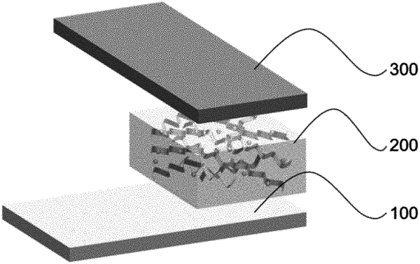
1. An electronic synaptic device comprising:
a lower electrode;
an upper electrode; and
an active layer provided between the lower electrode and the upper electrode and comprising a plurality of conductive nanoparticles,
wherein the conductive nanoparticles are dispersed in a matrix forming a continuous phase, and the matrix is composed of a protein,
wherein the protein is gelatin, and
wherein the electronic synaptic device is a nonvolatile memory device whose resistance changes according to an applied voltage.
|