| CPC H01L 43/04 (2013.01) [H01L 27/228 (2013.01); H01L 43/10 (2013.01); H01L 43/14 (2013.01)] | 20 Claims |
|
1. A semiconductor device, comprising:
a pair of transistors on a semiconductor substrate;
an interconnect structure over the pair of transistors, the interconnect structure comprising:
metal lines and vias over and connected to the pair of transistors;
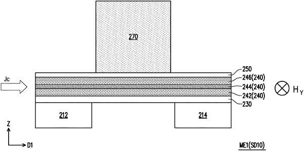
a composite spin Hall electrode over the metal lines and vias, the composite spin Hall electrode being electrically connected to the pair of transistors by the metal lines and vias, the composite spin Hall electrode comprising:
a first metal layer comprising a first heavy metal that includes a mixture of an α-β state;
a first spacer layer comprising a first material different from the first metal layer; and
a second metal layer over the first spacer layer, the second metal layer comprising the first heavy metal, wherein the first spacer layer is disposed between and in physical contact with the first metal layer and the second metal layer, and wherein the first spacer layer comprises an oxide; and
a magnetic tunnel junction over the composite spin Hall electrode.
|