| CPC H01L 51/006 (2013.01) [C07C 211/00 (2013.01); C07C 211/01 (2013.01); C07C 211/33 (2013.01); C07C 211/43 (2013.01); H01L 27/307 (2013.01); H01L 27/3206 (2013.01); H01L 51/0061 (2013.01); H01L 51/504 (2013.01); H01L 51/5064 (2013.01); H01L 51/5088 (2013.01); H01L 51/5096 (2013.01); H01L 51/5218 (2013.01); H01L 51/5221 (2013.01); H01L 51/5265 (2013.01); H01L 27/14612 (2013.01); H01L 27/322 (2013.01); H01L 51/0054 (2013.01); H01L 51/0055 (2013.01); H01L 51/0056 (2013.01); H01L 51/0058 (2013.01); H01L 51/0059 (2013.01); H01L 51/0072 (2013.01); H01L 51/5056 (2013.01); H01L 51/5072 (2013.01); H01L 2251/5315 (2013.01); H01L 2251/558 (2013.01)] | 15 Claims |
|
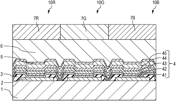
1. A light-emitting device comprising:
a reflection electrode;
a hole transport region;
a first luminescent layer being of an electron trapping type; and
a light extraction electrode, in this order,
wherein the hole transport region of the light-emitting device and a hole transport layer of another light-emitting device are disposed continuously;
wherein the first luminescent layer includes a first surface and a second surface closer to the light extraction electrode than the first surface, and
wherein a distance between the reflection electrode and the second surface of the first luminescent layer is equivalent to a length enabling emission from the first luminescent layer to be enhanced.
|