| CPC H01L 51/0097 (2013.01) [H01L 27/3244 (2013.01); H01L 51/56 (2013.01); H01L 2251/5338 (2013.01)] | 22 Claims |
|
1. A display apparatus comprising:
a first substrate;
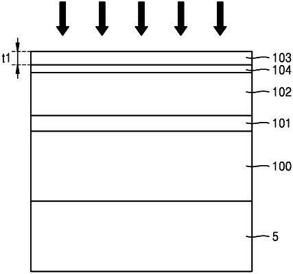
a conductive layer arranged on the first substrate doped with n-type impurities or p-type impurities;
a first barrier layer arranged on the conductive layer and doped with n-type impurities or p-type impurities; and
a semiconductor layer arranged on the first barrier layer, wherein
the conductive layer is doped with n-type impurities when the first barrier layer is doped with n-type impurities,
the conductive layer is doped with p-type impurities when the first barrier layer is doped with p-type impurities, and
the n-type impurities include one of phosphorous, fluorine, and nitrogen.
|