| CPC H01L 27/3223 (2013.01) [G09G 3/3225 (2013.01); H01L 27/3246 (2013.01); H01L 27/3276 (2013.01); H01L 51/105 (2013.01); H01L 51/5012 (2013.01); H01L 51/5056 (2013.01); H01L 51/5072 (2013.01); H01L 51/5092 (2013.01)] | 17 Claims |
|
1. A display apparatus, comprising:
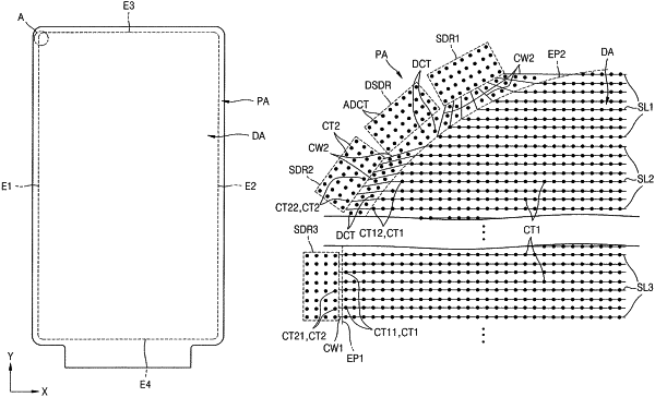
a substrate including a display area and a peripheral area outside the display area;
a first drive circuit located in the peripheral area, the first drive circuit to generate a scan signal and apply the scan signal to a thin film transistor that is located in the display area and is electrically connected to a pixel electrode;
a first insulating layer over the substrate in the display area and the peripheral area, the first insulating layer including a plurality of first contact holes located in the display area and a plurality of first dummy contact holes in the peripheral area such that the plurality of first dummy contact holes are located between the plurality of first contact holes and the first drive circuit; and
a second insulating layer disposed over the first insulating layer and filling the plurality of first dummy contact holes.
|