| CPC H01L 27/3223 (2013.01) [H01L 27/323 (2013.01); H01L 27/3258 (2013.01); H01L 27/3262 (2013.01); H01L 27/3265 (2013.01); H01L 27/3276 (2013.01); H01L 51/0031 (2013.01); H01L 51/5253 (2013.01); H01L 51/56 (2013.01); H01L 2227/323 (2013.01); H01L 2251/558 (2013.01)] | 13 Claims |
|
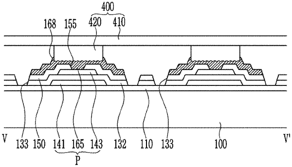
1. A display device comprising:
a substrate including a pad portion with a plurality of pads spaced apart from each other by a predetermined distance;
a flexible printed circuit board with a plurality of leads;
a semiconductor layer disposed on the substrate;
a gate insulating layer disposed on the semiconductor layer;
a gate electrode and a first capacitor electrode disposed on the gate insulating layer and spaced apart from each other;
a capacitor insulating layer disposed on the gate electrode and the first capacitor electrode;
a second capacitor electrode disposed on the capacitor insulating layer and overlapping the first capacitor electrode;
an interlayer insulating layer disposed on the capacitor insulating layer and the second capacitor electrode;
a source electrode and a drain electrode disposed on the interlayer insulating layer and spaced apart from each other;
a planarization film disposed on the source electrode and the drain electrode; and
a light emitting diode disposed on the planarization film and connected to the drain electrode,
wherein each of the plurality of pads is bonded to a corresponding lead of the plurality of leads, each of the plurality of pads includes a contact pad electrode that contacts a lower surface of the corresponding lead of the plurality of leads, and a dummy electrode surrounding a lower portion of the corresponding lead of the plurality of leads,
wherein the dummy electrode is directly connected to the contact pad electrode.
|