| CPC H01L 27/3218 (2013.01) [G06F 1/1624 (2013.01); G06F 1/1652 (2013.01); G06F 1/1681 (2013.01); H01L 27/3216 (2013.01); H01L 27/3276 (2013.01); H01L 51/0097 (2013.01); H01L 51/5048 (2013.01); H01L 51/5056 (2013.01); H01L 51/5072 (2013.01); H01L 51/5088 (2013.01); H01L 51/5092 (2013.01); H01L 51/5096 (2013.01); H01L 51/5212 (2013.01); H01L 51/5218 (2013.01); H01L 51/5253 (2013.01); H01L 51/5271 (2013.01)] | 11 Claims |
|
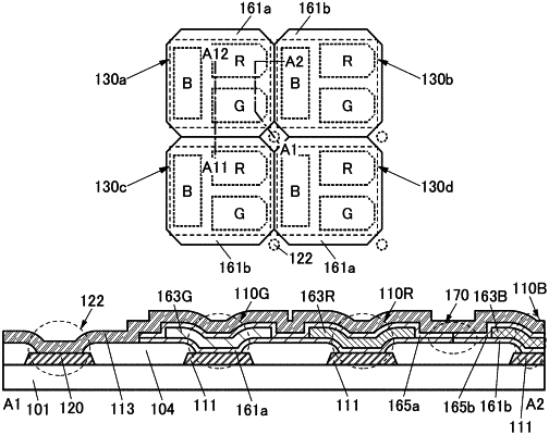
1. A display panel comprising:
a first pixel electrode;
a second pixel electrode;
a third pixel electrode;
a first light-emitting layer;
a second light-emitting layer;
a third light-emitting layer;
a first common layer;
a second common layer;
a common electrode; and
an auxiliary wiring,
wherein the first light-emitting layer is positioned over the first pixel electrode,
wherein the second light-emitting layer is positioned over the second pixel electrode,
wherein the third light-emitting layer is positioned over the third pixel electrode,
wherein the first light-emitting layer is configured to emit light of a color different from a color of light emitted from the second light-emitting layer,
wherein the first light-emitting layer is configured to emit light of a color identical to a color of light emitted from the third light-emitting layer,
wherein the first common layer is positioned over the first pixel electrode and the second pixel electrode,
wherein the first common layer comprises a portion overlapping with the first light-emitting layer and a portion overlapping with the second light-emitting layer,
wherein the second common layer is positioned over the third pixel electrode,
wherein the second common layer comprises a portion overlapping with the third light-emitting layer, and
wherein the common electrode comprises a portion overlapping with the first pixel electrode with the first common layer and the first light-emitting layer between the common electrode and the first pixel electrode, a portion overlapping with the second pixel electrode with the first common layer and the second light-emitting layer between the common electrode and the second pixel electrode, a portion overlapping with the third pixel electrode with the second common layer and the third light-emitting layer between the common electrode and the third pixel electrode, and a portion in contact with a top surface of the auxiliary wiring.
|