| CPC H01L 27/3276 (2013.01) [G06F 3/044 (2013.01); G06F 3/04164 (2019.05); H01L 51/5256 (2013.01); G06F 3/0412 (2013.01); G06F 3/0443 (2019.05); G06F 2203/04112 (2013.01); H01L 27/323 (2013.01)] | 20 Claims |
|
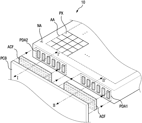
1. A display panel comprising:
a base layer in which a display area where a plurality of pixels are disposed and a non-display area surrounding the display area are defined;
a circuit element layer which is disposed on the base layer;
an input sensing layer which is disposed on the circuit element layer; and
a display signal pad and a sensing signal pad which are disposed on a sidewall,
wherein the sidewall is a single plane defined by each of the base layer, the circuit element layer, and the input sensing layer,
wherein the sidewall extends in a first direction which is perpendicular to a second direction, the second direction being a direction in which the base layer, the circuit element layer, and the input sensing layer are stacked,
wherein the sidewall comprises a first pad area and a second pad area which is separated from the first pad area, the first pad area and the second pad area being arranged in the first direction,
wherein the display signal pad is electrically coupled to a display signal line disposed in the circuit element layer, and the sensing signal pad is electrically coupled to an input sensing line disposed in the input sensing layer,
wherein the display signal pad is disposed in the first pad area, and
wherein the sensing signal pad is disposed in the second pad area.
|