| CPC H01L 27/3272 (2013.01) [B23K 26/04 (2013.01); B23K 26/0617 (2013.01); B23K 26/0622 (2015.10); B23K 26/0643 (2013.01); B23K 26/0648 (2013.01); B23K 26/083 (2013.01); H01L 27/1225 (2013.01); H01L 27/1266 (2013.01); H01L 27/322 (2013.01); H01L 27/3258 (2013.01); H01L 27/3262 (2013.01); H01L 29/24 (2013.01); H01L 29/66969 (2013.01); H01L 29/7869 (2013.01); H01L 29/78603 (2013.01); H01L 51/003 (2013.01); H01L 51/0024 (2013.01); H01L 51/0027 (2013.01); H01L 51/0097 (2013.01); H01L 51/5246 (2013.01); H01L 51/5253 (2013.01); H01L 51/56 (2013.01); H01L 27/3244 (2013.01); H01L 41/314 (2013.01); H01L 51/5096 (2013.01); H01L 51/5284 (2013.01); H01L 2227/323 (2013.01); H01L 2227/326 (2013.01); H01L 2251/5338 (2013.01); H01L 2251/558 (2013.01); Y02E 10/549 (2013.01); Y02P 70/50 (2015.11)] | 16 Claims |
|
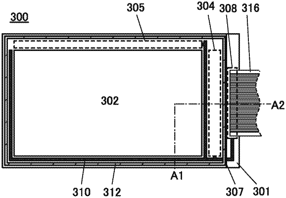
1. An electronic device comprising:
a first flexible substrate;
a first bonding layer over the first flexible substrate;
a first organic resin layer over the first bonding layer;
an insulating layer over the first organic resin layer;
a transistor over the insulating layer;
an organic electroluminescent element electrically connected to the transistor;
a touch sensor over the organic electroluminescent element;
a second organic resin layer over the organic electroluminescent element;
a second bonding layer over the second organic resin layer; and
a second flexible substrate over the second bonding layer,
wherein a thickness of the first organic resin layer is less than or equal to 20 μm, and
wherein at least a part of the electronic device is curved.
|