| CPC H01L 27/3246 (2013.01) [H01L 27/3283 (2013.01); H01L 51/56 (2013.01)] | 17 Claims |
|
1. A display substrate, comprising:
a base substrate;
a plurality of first electrodes arranged in an array on the base substrate; and
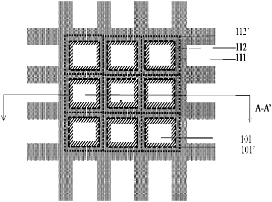
a pixel defining layer defining a plurality of openings on the base substrate; the plurality of openings overlapping the plurality of first electrodes respectively;
wherein the pixel defining layer comprises a plurality of first pixel defining units and a plurality of second pixel defining units, and the plurality of second pixel defining units are disposed on the plurality of first pixel defining units;
the plurality of first pixel defining units are separated from one another; and
orthographic projections of the plurality of first pixel defining units on the base substrate fall within orthographic projections of the plurality of first electrodes on the base substrate respectively, and the plurality of second pixel defining units cover sidewalls of the plurality of first electrodes and separate adjacent first electrodes.
|