| CPC H01L 27/3262 (2013.01) [H01L 27/323 (2013.01); G09G 3/3233 (2013.01); G09G 2300/0426 (2013.01); H01L 27/1222 (2013.01); H01L 27/1274 (2013.01); H01L 29/66757 (2013.01); H01L 29/78675 (2013.01); H01L 2227/323 (2013.01)] | 13 Claims |
|
1. A display device comprising:
a substrate; and
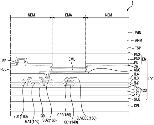
a semiconductor layer disposed on the substrate, and comprising a first area, a second area, and a third area that are sequentially positioned by dividing the semiconductor layer into three areas in a thickness direction of the semiconductor layer,
wherein the semiconductor layer comprises polycrystalline silicon,
a concentration of fluorine contained in the semiconductor layer has a first peak value in the first area and a second peak value in the third area, and
the first peak value of the concentration of the fluorine in the semiconductor layer is about 30% or less of the second peak value of the concentration of the fluorine in the semiconductor layer.
|