| CPC H10B 63/845 (2023.02) [H01L 21/31116 (2013.01); H01L 21/7682 (2013.01); H10B 41/27 (2023.02); H10B 43/27 (2023.02)] | 19 Claims |
|
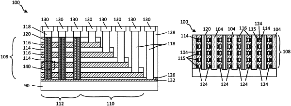
1. An integrated circuit comprising:
a vertical layer stack of alternating layers of a conductive material and an insulating material, the stack including an insulating material layer between first and second neighboring conductive material layers; and
an isolation material along a side of the layer stack, the isolation material compositionally distinct from the insulating material;
wherein the insulating material layer has a lateral width that is shorter than a lateral width of the first and second neighboring conductive material layers such that the layer stack defines a void between the first and second neighboring conductive material layers, the void further located between the isolation material and the insulating material.
|