| CPC H01L 27/249 (2013.01) [H01L 45/1233 (2013.01); H01L 45/06 (2013.01); H01L 45/144 (2013.01)] | 20 Claims |
|
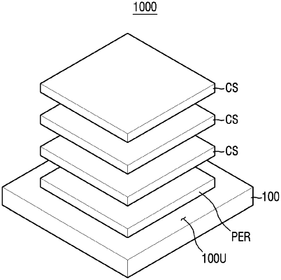
1. A variable resistance memory device comprising:
lower conductive lines extending in a first direction on a substrate and spaced apart from each other in a second direction crossing the first direction;
peripheral transistors on the substrate and arranged under the lower conductive lines in a third direction crossing the first direction and the second direction; and
lower contacts electrically connecting the lower conductive lines to the peripheral transistors and extending in the third direction,
wherein each of the lower conductive lines comprises a first lower extending portion extending in the first direction, a second lower extending portion offset in the second direction from the first lower extending portion and extending in the first direction, and a lower connecting portion that couples the first lower extending portion to the second lower extending portion, and
wherein each of the lower contacts is on the lower connecting portion of a respective one of the lower conductive lines.
|