| CPC H01L 27/2481 (2013.01) [H01L 27/2454 (2013.01); H01L 45/06 (2013.01); H01L 45/1253 (2013.01); H01L 45/144 (2013.01); H01L 45/146 (2013.01); H01L 45/16 (2013.01)] | 20 Claims |
|
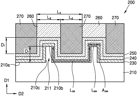
1. A memory device comprising:
an insulating structure including a first surface and a protrusion portion protruding from the first surface in a first direction;
a recording material layer on the insulating structure, the recording material layer extending along a protruding surface of the protrusion portion to cover the protrusion portion and extending onto the first surface of the insulating structure;
a channel layer on the recording material layer and extending along a surface of the recording material layer;
a gate insulating layer on the channel layer; and
a gate electrode on the gate insulating layer at a location facing a second surface of the insulating structure, the second surface of the insulating structure being a protruding upper surface of the protrusion portion.
|