| CPC H01L 27/2481 (2013.01) [H01L 27/2427 (2013.01); H01L 45/06 (2013.01); H01L 45/1233 (2013.01); H01L 45/143 (2013.01); H01L 45/144 (2013.01); H01L 45/1675 (2013.01)] | 20 Claims |
|
1. A semiconductor device comprising:
a first conductive line extending on a substrate in a first horizontal direction, the first horizontal direction being parallel to a first upper surface of the substrate;
a second conductive line extending on the first conductive line in a second horizontal direction, the second horizontal direction being parallel to the first upper surface of the substrate and perpendicular to the first horizontal direction;
a first memory cell structure between the first conductive line and the second conductive line;
a lower interlayer insulating layer adjacent to a first side of the first memory cell structure;
a lower capping layer between the first memory cell structure and the lower interlayer insulating layer; and
a lower spacer between the lower capping layer and a portion of the first side of the first memory cell structure,
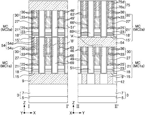
wherein the first memory cell structure includes a first lower electrode pattern, a first switching material pattern, a first intermediate electrode pattern, a first data storage material pattern, and a first upper electrode pattern that are sequentially stacked,
the first intermediate electrode pattern includes a first intermediate conductive layer and a second intermediate conductive layer that are sequentially stacked,
the first upper electrode pattern includes a first upper conductive layer and a second upper conductive layer that are sequentially stacked,
at least one of the first lower electrode pattern, the first intermediate conductive layer, or the second upper conductive layer includes a first material layer, the first material layer including at least one of a first carbon material layer or a first carbon-containing material layer, and
the first material layer includes a first region doped with nitrogen and a second region that is not doped with the nitrogen or is doped with the nitrogen at a first concentration lower than a second concentration of the nitrogen in the first region.
|