| CPC H01L 27/11507 (2013.01) [H01L 27/24 (2013.01); H01L 29/516 (2013.01)] | 18 Claims |
|
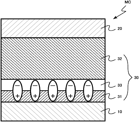
1. A memory device comprising:
a first conductive layer;
a second conductive layer;
a ferroelectric layer provided between the first conductive layer and the second conductive layer and containing hafnium oxide;
a paraelectric layer provided between the first conductive layer and the ferroelectric layer and containing a first oxide; and
an oxide layer provided between the ferroelectric layer and the second conductive layer, the oxide layer being in contact with the ferroelectric layer, and containing a second oxide having an oxygen area density lower than an oxygen area density of hafnium oxide.
|