| CPC H01L 27/11568 (2013.01) [H01L 27/11565 (2013.01); H01L 27/11582 (2013.01)] | 11 Claims |
|
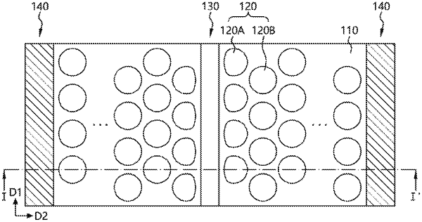
1. A semiconductor memory device comprising:
an electrode structure including insulating interlayers and gate conductive layers which are alternately stacked;
a plurality of channel posts formed to pass through the electrode structure; and
at least one gate separation layer arranged between the channel posts to separate an uppermost gate conductive layer among the gate conductive layers in the electrode structure,
wherein among the plurality of channel posts, channel posts adjacent to the gate separation layer have a first curved portion and a second curved portion having different curvatures in a planar view.
|