US 11,672,120 B2
Integrated assemblies having charge-trapping material arranged in vertically-spaced segments, and methods of forming integrated assemblies
Byeung Chui Kim, Boise, ID (US); Francois H. Fabreguette, Boise, ID (US); Richard J. Hill, Boise, ID (US); Purnima Narayanan, Boise, ID (US); and Shyam Surthi, Boise, ID (US)
Assigned to Micron Technology, Inc., Boise, ID (US)
Filed by Micron Technology, Inc., Boise, ID (US)
Filed on May 24, 2021, as Appl. No. 17/328,237.
Application 17/328,237 is a continuation of application No. 16/988,548, filed on Aug. 7, 2020, granted, now 11,037,956.
Application 16/988,548 is a continuation of application No. 16/374,527, filed on Apr. 3, 2019, granted, now 10,777,576, issued on Sep. 15, 2020.
Prior Publication US 2021/0327898 A1, Oct. 21, 2021
This patent is subject to a terminal disclaimer.
Int. Cl. H01L 27/11582 (2017.01); H01L 21/02 (2006.01); H01L 27/1157 (2017.01); G11C 16/08 (2006.01)
CPC H01L 27/11582 (2013.01) [G11C 16/08 (2013.01); H01L 21/0214 (2013.01); H01L 27/1157 (2013.01)] 19 Claims
OG exemplary drawing
 
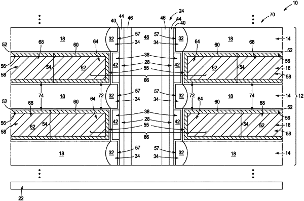
1. A memory array, comprising:
a vertical stack of alternating insulative levels and conductive wordlines; the insulative levels having terminal ends comprising first insulative material;
a charge-blocking material extending vertically along the stack;
a charge-storage material being configured as first segments which are arranged one atop another, and which are vertically spaced from one another by intervening second segments comprising the first insulative material within the terminal ends;
a charge-tunneling material adjacent to the charge-storage material; and
a channel material extending vertically along the stack.