| CPC H01L 27/11582 (2013.01) [G11C 7/18 (2013.01); H01L 23/5226 (2013.01); H01L 27/11565 (2013.01)] | 20 Claims |
|
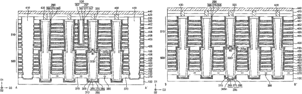
1. A vertical memory device comprising:
a gate electrode structure on a substrate and including gate electrodes spaced apart in a first direction;
channels extending through the gate electrode structure and including a first portion on the substrate and a second portion contacting the first portion, wherein the second portion includes a lower surface having a width less than a width of an upper surface of the first portion;
a charge storage structure covering an outer sidewall of each of the channels;
a first dummy channel extending through the gate electrode structure and spaced apart from the channels, wherein the first dummy channel includes a third portion on the substrate and a fourth portion contacting the third portion and the fourth portion includes a lower surface having a width less than a width of an upper surface of the third portion; and
a division pattern extending between the channels in a second direction, wherein the division pattern includes a second dummy channel and a second dummy charge storage structure covering a sidewall and a lower surface of the second dummy channel, wherein:
the second dummy channel contacts an upper outer sidewall of the fourth portion of the first dummy channel,
the second dummy channel includes a material substantially the same as each of the channels, and
the second dummy charge storage structure includes a material substantially the same as the charge storage structure.
|
|
11. A vertical memory device comprising:
a gate electrode structure on a substrate and including gate electrodes spaced apart in a first direction;
channels extending through the gate electrode structure and including a first portion on the substrate and a second portion contacting the first portion, wherein the second portion includes a lower surface having a width less than a width of an upper surface of the first portion;
a first dummy channel extending through the gate electrode structure and spaced apart from the channels, wherein the first dummy channel includes a third portion on the substrate and a fourth portion contacting the third portion and the fourth portion includes a lower surface having a width less than a width of an upper surface of the third portion; and
a division pattern extending in a second direction between the channels and including a second dummy channel and a second dummy charge storage structure covering a sidewall and a lower surface of the second dummy channel, wherein:
the first dummy channel includes a material substantially the same as each of the channels,
the first dummy channel includes a protrusion portion protruding in the first direction from a lower surface of the third portion and a lowermost surface is lower than a lowermost surface of each of the channels, and
the second dummy channel contacts an upper outer sidewall of the first dummy channel.
|
|
18. A vertical memory device comprising:
a gate electrode structure on a substrate and including gate electrodes spaced apart in a first direction;
channels extending through the gate electrode structure and including a first portion on the substrate and a second portion contacting the first portion and the second portion includes a lower surface having a width less than a width of an upper surface of the first portion;
a charge storage structure covering an outer sidewall of each of the channels;
a first dummy channel extending through the gate electrode structure and spaced apart from the channels, wherein the first dummy channel includes a third portion on the substrate and a fourth portion contacting the third portion and the fourth portion includes a lower surface having a width less than a width of an upper surface of the third portion;
a first dummy charge storage structure covering an outer sidewall of the first dummy channel;
a division pattern extending between the channels in a second direction and including a second dummy channel;
a second dummy charge storage structure covering a sidewall and a lower surface of the second dummy channel;
contact plugs respectively on the channels; and
a bit line extending in a third direction and electrically connected to the contact plugs, wherein:
each of the first dummy channel and the second dummy channel includes a material substantially the same as the channels,
each of the first dummy charge storage structure and the second dummy charge storage structure includes a material substantially the same as the charge storage structure,
the second dummy channel contacts an upper outer sidewall of the first dummy channel, and
the second dummy charge storage structure contacts an upper outer sidewall of the first dummy charge storage structure.
|