| CPC H01L 27/11556 (2013.01) [G11C 5/025 (2013.01); G11C 5/06 (2013.01); H01L 27/11582 (2013.01)] | 19 Claims |
|
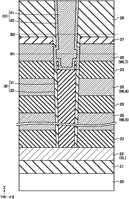
1. A semiconductor storage device comprising:
a substrate having a surface;
a first conductive layer disposed on the substrate, the first conductive layer extending in a first direction parallel to the surface of the substrate, the first conductive layer having a hole extending through the first conductive layer;
a second conductive layer disposed on over the first conductive layer, and extending in the first direction;
a first insulating layer disposed between the first conductive layer and the second conductive layer,
a first insulation plug disposed on the substrate, the first insulation plug extending in a second direction intersecting with the first direction, the first insulation plug extending through the hole of the first conductive layer; and
a contact plug disposed on the first insulation plug, the contact plug extending in the second direction, and intersecting with the second conductive layer,
wherein a first width of the hole of the first conductive layer in the first direction is substantially the same as a second width of the first insulation plug at the first insulating layer in the first direction,
wherein a corner between the hole and an upper surface of the second conductive layer is covered with a second insulating layer.
|