| CPC H01L 27/11556 (2013.01) [G11C 5/025 (2013.01); G11C 5/06 (2013.01); G11C 16/0408 (2013.01); G11C 16/0466 (2013.01); G11C 16/0483 (2013.01); H01L 27/11582 (2013.01)] | 17 Claims |
|
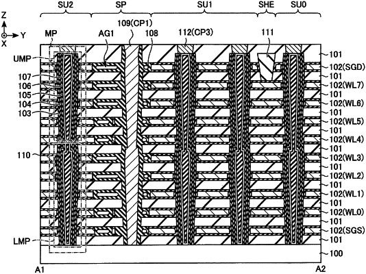
1. A semiconductor memory device comprising:
a plurality of first insulating layers arranged apart from each other in a first direction;
a plurality of first interconnect layers stacked alternately with the first insulating layers, and extending in a second direction intersecting the first direction;
a plurality of second interconnect layers stacked alternately with the first insulating layers, arranged adjacently to the first interconnect layers in a third direction intersecting the first and second directions, and extending in the second direction;
a plurality of first semiconductor layers extending in the first direction and passing through the first interconnect layers and the first insulating layers;
a plurality of second semiconductor layers extending in the first direction and passing through the second interconnect layers and the first insulating layers; and
a separation region including a plurality of first portions and a plurality of second portions, the first portions extending in the first direction, passing through the first insulating layers, being provided between the first interconnect layers and the second interconnect layers, and being arranged apart from each other in the second direction, the second portions being provided between the first interconnect layers and the second interconnect layers, and protruding from an outer periphery of each of the first portions, wherein
the second portions protruding from adjacent ones of the first portions are linked to each other,
the first interconnect layers and the second interconnect layers are separated from each other in the third direction by the first portions and the linked second portions, and
a first length between centers of two adjacent ones of the first portions is less than double a second length from a center of one of the first portions to an outer periphery of one of the second portions corresponding to the one of the first portions, in a cross section intersecting the first direction and including one of the first interconnect layers and one of the second interconnect layers.
|