| CPC H05K 3/18 (2013.01) [C25D 5/022 (2013.01); C25D 7/00 (2013.01); C25D 17/008 (2013.01); H05K 3/108 (2013.01); H05K 2203/0723 (2013.01)] | 13 Claims |
|
1. A printed wiring board production method that foiiiis a conductive pattern on a base film by an additive method or a subtractive method, comprising:
a plating process that electroplates the conductive pattern on a surface of the base film, wherein
the plating process includes
a shield plate arranging process that arranges a shield plate between an anode and a printed wiring board substrate that forms a cathode,
a substrate arranging process that arranges the printed wiring board substrate in a plating tank by a jig that holds the printed wiring board substrate, and
an anode shield plate arranging process that arranges an anode shield plate between the shield plate and the anode at a position separated from the shield plate and the anode,
a distance between the shield plate and the printed wiring board substrate is 50 mm or greater but 150 mm or less,
a distance between the anode shield plate and the printed wiring board substrate is 100 mm or greater but 300 mm or less,
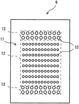
the shield plate includes an opening region opposing the printed wiring board substrate in a plan view, and shield plate openings formed in an array within the opening region,
the opening region includes a rectangular central region at a center portion of the opening region, and a pair of rectangular end regions at end portions on opposite sides of the central region,
the rectangular central region does not overlap the pair of rectangular end regions in the plan view, and
an opening ratio of the rectangular central region of the opening region is different from an opening ratio of each of the pair of rectangular end regions of the opening region.
|