| CPC H05B 45/325 (2020.01) [G01S 7/484 (2013.01); G05F 1/56 (2013.01); H05B 45/30 (2020.01); H05B 47/25 (2020.01)] | 21 Claims |
|
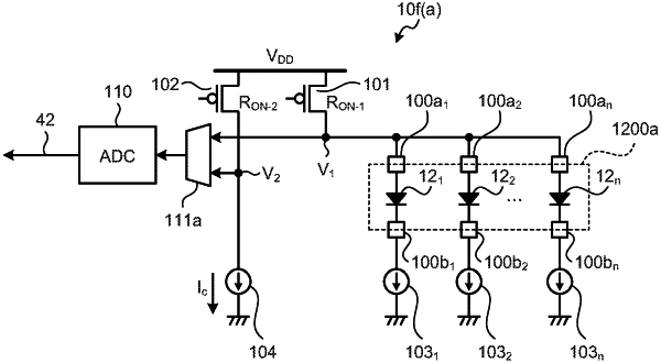
1. A light source device, comprising:
a first resistor connected to a potential;
a light emitting element connected in series to the first resistor;
a second resistor connected to the potential;
a first current source connected in series to the second resistor, wherein the first current source is configured to supply a freely-selected current;
a first connection part where the first resistor is connected to the light emitting element, wherein the first connection part is configured to output a first voltage;
a second connection part where the second resistor is connected to the first current source, wherein the second connection part is configured to output a second voltage; and
a detector configured to detect a first drive current for the light emitting element, wherein the detection of the first drive current is based on the first voltage, the second voltage, and the freely-selected current.
|