| CPC H04N 5/374 (2013.01) [H01L 27/14621 (2013.01); H01L 27/14627 (2013.01); H01L 27/14643 (2013.01); H04N 5/341 (2013.01)] | 19 Claims |
|
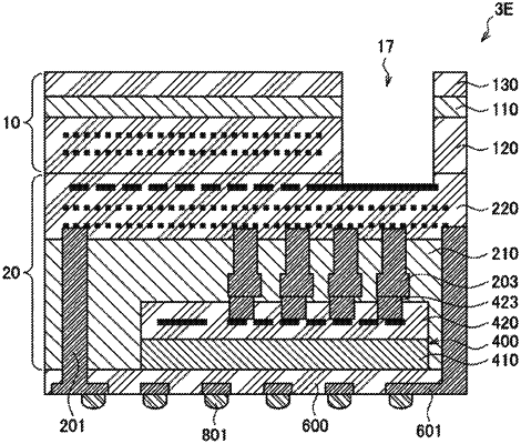
1. A solid-state imaging device, comprising:
a first substrate that includes:
a principal surface; and
a pixel portion on the principal surface, wherein the pixel portion includes a plurality of pixels;
a second substrate that includes:
a first surface in contact with the first substrate;
a second surface opposite to the first surface;
an opening in a partial region on the second surface of the second substrate;
at least one sub-chip inside the opening, wherein the at least one sub-chip includes a first circuit configured to execute a first function; and
a first multi-layer wiring layer on the sub-chip and the second substrate, wherein
the first multi-layer wiring layer covers the opening,
the first multi-layer wiring layer includes an external input/output terminal, and
the external input/output terminal overlaps at least one of the second substrate or the at least one sub-chip.
|