| CPC H04N 25/745 (2023.01) [H01L 27/14612 (2013.01); H01L 27/14643 (2013.01); H01L 27/14856 (2013.01); H04N 25/533 (2023.01)] | 20 Claims |
|
1. An image sensor comprising:
an image sensor pixel array; and
row control circuitry coupled to the image sensor pixel array, the row control circuitry including:
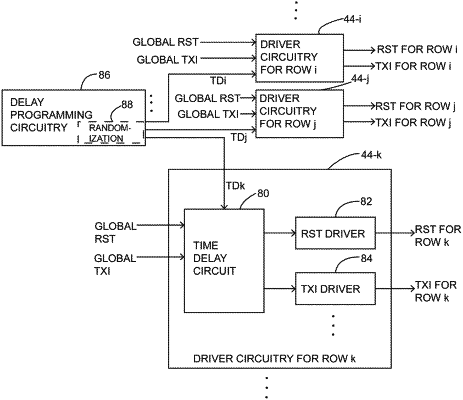
a first control signal driver circuit coupled to a pixel row in the image sensor pixel array;
a second control signal driver circuit coupled to the pixel row;
timing control circuitry coupled to the first and second control signal driver circuits; and
a time delay circuit coupled between the first control signal driver circuit and the timing control circuitry and coupled between the second control signal driver circuit and the timing control circuitry, wherein the time delay circuit receives a global timing control signal as a first input and a clock signal as a second input and outputs a delayed version of the global timing control signal by introducing a time delay to the global timing control signal and wherein the first control signal driver circuit receives the delayed version of the global timing control signal.
|