| CPC H04N 25/702 (2023.01) [G01S 17/08 (2013.01); H04N 25/77 (2023.01)] | 12 Claims |
|
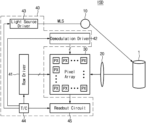
1. An image sensing device comprising:
an image sensing pixel array comprising a plurality of image sensing pixels formed in a substrate, each image sensing pixel including a first electrical contact tap and a second electrical contact tap structured to generate a current in the substrate and capture photocharges generated by light reflected from an object and incident on the image sensing pixel array and migrating by the current to measure a distance to the object by performing demodulation operations based on the photocharges; and
a demodulation driver coupled to the image sensing pixel array to apply, to the first electrical contact tap and the second electrical contact tap, a first demodulation control signal and a second demodulation control signal for generating the current, respectively,
wherein the plurality of image sensing pixels includes first and second image sensing pixels, and wherein a distance between the first image sensing pixel and the demodulation driver is smaller than a distance between the second image sensing pixel and the demodulation driver, and wherein the first image sensing pixel is structured to have a larger resistance than the second image sensing pixel,
wherein the first electrical contact tap comprises a first control node structured to receive the first demodulation control signal and a first detection node structured to capture the photocharges, and
the second electrical contact tap comprises a second control node structured to receive the second demodulation control signal and a second detection node structured to capture the photocharges, and
wherein the first control node of the first image sensing pixel has a smaller depth than the first control node of the second image sensing pixel.
|