US 11,671,721 B2
Solid-state imaging device, method of manufacturing solid-state imaging device, and electronic apparatus
Hiroaki Ishiwata, Tokyo (JP)
Assigned to SONY SEMICONDUCTOR SOLUTIONS CORPORATION, Kanagawa (JP)
Filed by Sony Semiconductor Solutions Corporation, Kanagawa (JP)
Filed on Mar. 10, 2021, as Appl. No. 17/197,203.
Application 17/197,203 is a continuation of application No. 16/779,068, filed on Jan. 31, 2020, granted, now 10,978,506.
Application 16/779,068 is a continuation of application No. 16/204,194, filed on Nov. 29, 2018, granted, now 10,720,458, issued on Jul. 21, 2020.
Application 16/204,194 is a continuation of application No. 16/031,345, filed on Jul. 10, 2018, granted, now 10,177,184, issued on Jan. 8, 2019.
Application 16/031,345 is a continuation of application No. 15/894,542, filed on Feb. 12, 2018, granted, now 10,050,073, issued on Aug. 14, 2018.
Application 15/894,542 is a continuation of application No. 15/465,084, filed on Mar. 21, 2017, granted, now 9,923,005, issued on Mar. 20, 2018.
Application 15/465,084 is a continuation of application No. 15/156,564, filed on May 17, 2016, granted, now 9,653,499, issued on May 16, 2017.
Application 15/156,564 is a continuation of application No. 14/495,318, filed on Sep. 24, 2014, granted, now 9,438,833, issued on Sep. 6, 2016.
Application 14/495,318 is a continuation of application No. 13/085,676, filed on Apr. 13, 2011, abandoned.
Claims priority of application No. 2010-107265 (JP), filed on May 7, 2010.
Prior Publication US 2021/0195127 A1, Jun. 24, 2021
Int. Cl. H04N 25/60 (2023.01); H01L 27/146 (2006.01); H04N 23/10 (2023.01); H04N 23/54 (2023.01); H04N 23/55 (2023.01); H04N 25/46 (2023.01); H04N 25/70 (2023.01); H04N 25/77 (2023.01); H04N 25/13 (2023.01); H04N 25/702 (2023.01); H04N 25/778 (2023.01)
CPC H04N 25/60 (2023.01) [H01L 27/14603 (2013.01); H01L 27/14605 (2013.01); H01L 27/14612 (2013.01); H01L 27/14621 (2013.01); H01L 27/14627 (2013.01); H01L 27/14641 (2013.01); H01L 27/14645 (2013.01); H01L 27/14647 (2013.01); H01L 27/14685 (2013.01); H04N 23/10 (2023.01); H04N 23/54 (2023.01); H04N 23/55 (2023.01); H04N 25/134 (2023.01); H04N 25/46 (2023.01); H04N 25/70 (2023.01); H04N 25/702 (2023.01); H04N 25/77 (2023.01); H04N 25/778 (2023.01)] 17 Claims
OG exemplary drawing
 
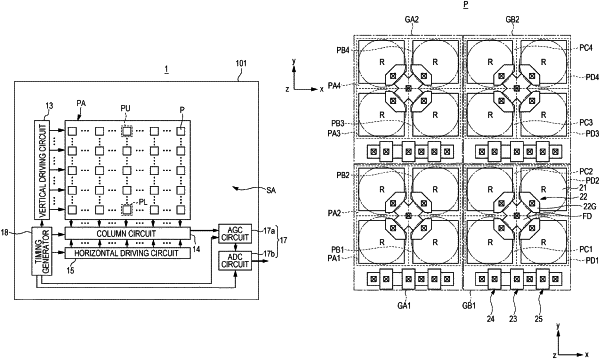
1. A light detecting device comprising a plurality of unit pixels, wherein each of the unit pixels includes:
a plurality of first photoelectric conversion portions;
a plurality of first transfer gates;
a first floating diffusion region;
a plurality of second photoelectric conversion portions;
a plurality of second transfer gates; and
a second floating diffusion region,
wherein,
the first photoelectric conversion portions and the second photoelectric conversion portions are configured to receive and convert light of the same color,
each of the first transfer gates is configured to transfer a signal charge in a respective one of the first photoelectric conversion portions to the first floating diffusion region, and
each of the second transfer gates is configured to transfer a signal charge in a respective one of the second photoelectric conversion portions to the second floating diffusion region.