| CPC H04N 23/72 (2023.01) [H04N 23/71 (2023.01)] | 18 Claims |
|
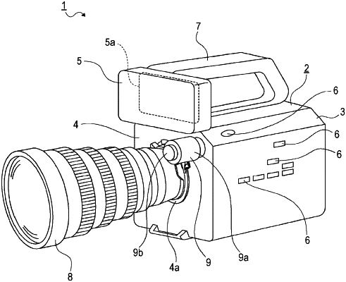
1. An imaging apparatus, comprising:
a variable neutral density filter that has a variable transmittance;
an imaging device including a sensor on which object light via the variable neutral density filter forms an image;
variable transmittance drive circuitry configured to change a transmittance of the variable neutral density filter in accordance with a transmittance control value;
a hardware input device that can be in a first state or in a second state depending on a change in form; and
transmittance designation circuitry configured to set a transmittance control value directed to the variable transmittance drive circuitry in accordance with an operation amount of the hardware input device when the hardware input device is in the first state, and select one transmittance control value from among a plurality of transmittance control values in accordance with an operation of the hardware input device and set the one transmittance control value as the transmittance control value directed to the variable transmittance drive circuitry when the hardware input device is in the second state, the plurality of transmittance control values being stored in a preset memory.
|