| CPC H04N 5/33 (2013.01) [B60R 11/04 (2013.01); H04N 5/23241 (2013.01); H04N 17/002 (2013.01); B60R 2011/0026 (2013.01); B60R 2300/10 (2013.01)] | 21 Claims |

|
1. An imaging device, comprising:
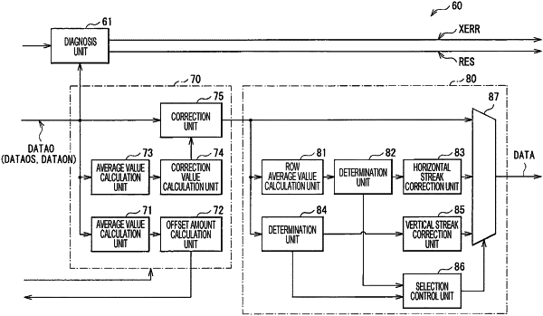
an imaging sensor including a pixel array and a processor, the processor being configured to process a pixel signal corresponding to an image captured by the pixel array to generate an image signal and a diagnostic signal based on the pixel signal, the image signal and the diagnostic signal comprising image data of the pixel signal;
a diagnosis circuit configured to perform diagnosis processing for the imaging sensor based on the diagnostic signal; and
an output circuit configured to output a flag signal corresponding to a result of the diagnosis processing, wherein:
the flag signal is set to a ground level signal if the result of the diagnosis processing indicates an error,
the flag signal is changeable between the ground level signal and a first signal corresponding to a first power supply voltage, and
the output circuit is configured to output the first signal during a first period after an activation time corresponding to when the imaging device is changed to a powered on state, and the output circuit is configured to output the ground level signal during a second period after the first period.
|