| CPC H04B 1/40 (2013.01) [H03F 3/245 (2013.01); H03H 11/28 (2013.01); H03F 2200/294 (2013.01); H03F 2200/451 (2013.01)] | 23 Claims |
|
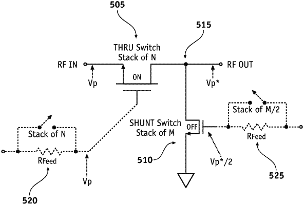
1. A circuital arrangement comprising:
a combination of a series RF switch and a shunt RF switch, the series RF switch connected between a first RF terminal and a second RF terminal, the shunt RF switch connected between the second RF terminal and ground, the shunt RF switch configured to be in an ON steady state when the series RF switch is in an OFF steady state and vice versa, each of the series RF switch and the shunt RF switch comprising a stacked arrangement of respective N and M FET switches; and
a plurality of series gate feed arrangements coupled to gates of the FET switches of the series RF switch, and one or more shunt gate feed arrangements coupled to gates of the FET switches of the shunt RF switch, each series gate feed arrangement and shunt gate feed arrangement comprising respective K and L bypass switches connected across one or more common gate resistors, wherein L is less than M.
|