| CPC H03L 7/1976 (2013.01) [H03K 19/20 (2013.01); H03L 7/0816 (2013.01); H03L 7/0818 (2013.01); H03L 7/199 (2013.01)] | 17 Claims |
|
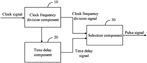
1. A pulse signal generation circuit, comprising:
a clock frequency division component, wherein an input end of the clock frequency division component receives a clock signal, and the clock frequency division component is configured to perform frequency division on the clock signal to generate a clock frequency division signal;
a time delay component, wherein an input end of the time delay component is connected to an output end of the clock frequency division component, and the time delay component is configured to generate a time delay signal based on the clock frequency division signal; and
a selection component, wherein input ends of the selection component are respectively connected to the output end of the clock frequency division component and an output end of the time delay component, and the selection component is configured to receive the clock frequency division signal and the time delay signal at the same time, and perform selection on the clock frequency division signal and the time delay signal according to a preset condition to generate a pulse signal.
|