| CPC H03K 17/6872 (2013.01) [H03K 2217/0063 (2013.01); H03K 2217/0072 (2013.01)] | 26 Claims |
|
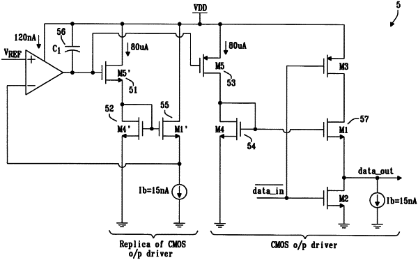
1. A driver circuit configured to generate an output voltage at an output terminal of the driver circuit, the driver circuit comprising
a high side switching element coupled between a supply terminal and the output terminal of the driver circuit,
a low side switching element coupled between the output terminal of the driver circuit and a reference potential,
a regulation transistor, wherein a controlled section of the regulation transistor is coupled in series with the high side switching element and the low side switching element between the supply terminal and the reference potential, and
a feedback circuit configured to regulate the output voltage by generating a regulation voltage at a control terminal of the regulation transistor,
wherein an input voltage of the driver circuit is applied to both a control terminal of the high side switching element and to a control terminal of the low side switching element.
|