| CPC H03K 5/1565 (2013.01) [H03K 5/13 (2013.01); H03K 19/20 (2013.01); H03K 2005/00019 (2013.01)] | 20 Claims |
|
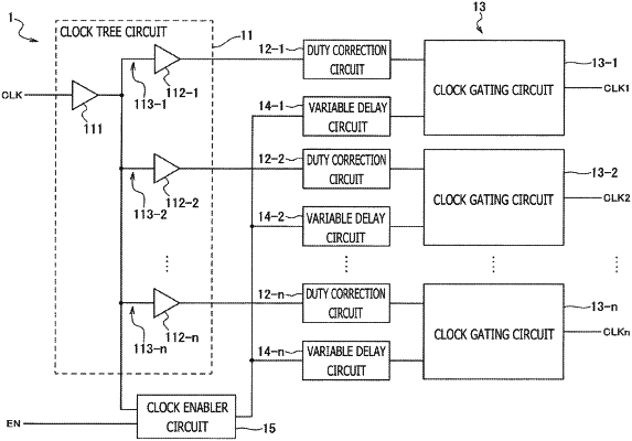
1. A circuit system comprising:
a clock tree circuit that has multiple lanes to which a clock signal is distributed;
a duty correction circuit that is provided on each of the multiple lanes and corrects a duty ratio of the clock signal;
a clock gating circuit group having a clock gating circuit that is provided on each of the multiple lanes and receives, as input, the clock signal from the duty correction circuit, the clock gating circuit group starting output of the clock signal from each of a plurality of the clock gating circuits in a predetermined period; and
a variable delay circuit that is provided in association with each of a plurality of the duty correction circuits and is capable of changing a delay time of a control signal that controls a timing of starting output of the clock signal from the clock gating circuit.
|